Model Name :
Zeiss Gemini SEM 450
SPECIFICATION
- Resolution: 0.7 nm @ 15 kV, 1.1 nm @ 1kV/500 V , 1.5 nm @ 200 Volt
- Accelerating voltage: 20 V to 30 kV
- Beam current : 10 pA to 300 nA
- Magnification: 12 – 2,000,000x
- Working distance 0.1 – 50 mm
- Detectors:
- In-lens, SE, BSD
- EDS (Energy Dispersive x-ray Spectroscopy) for composition analysis
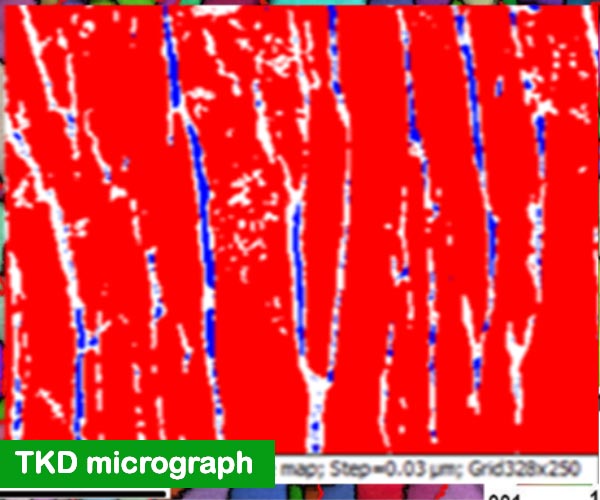
- High-speed High-Resolution EBSD (Electron backscattered diffraction) detector which enables the detailed orientation imaging microscopy analysis
- TKD (Transmission Kikuchi Diffraction) facility is available and can be performed on TEM samples.
Applications FESEM is applicable for
- Micro/Nanostructural analysis
- Elemental analysis
- Phase and orientation relationship analysis
- Crystallographic texture analysis
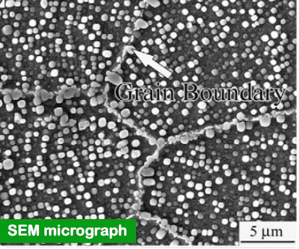
- Morphology and grain analysis
- Grain boundary engineering, metallurgical & materials Study
- Failure analysis
 |
 |
 |
Features and Capabilities:
- Gemini SEM 450 is having highest performance analytics and ultra-high resolution capabilities for comprehensive nano-scale imaging and analysis
- The unique combination of proven GEMINI II column and detection technology delivers leading image contrasts for comprehensive sample characterization.
- Straightforward and Outstanding Ultra Large Field Imaging
- Magnetic sample imaging at all working distances.
- The optimized objective lens delivers outstanding resolution over ultra large fields of view
- EDAX TEAM Pegasus Integrated EDS-EBSD system having Octane Elect Plus Silicon Drift Detector with OIM software for detailed image analysis.
- The Pegasus Analysis System enables the simultaneous collection of Energy Dispersive Spectroscopy (EDS) (chemistry) and Electron Backscatter Diffraction (EBSD) (crystallography) data, allowing direct correlation between the elemental content and microstructural aspects of the material being studied.
- The Octane Elect EDS System is an enhanced Energy Dispersive Spectroscopy (EDS) platform that provides excellent resolution and high throughput at an optimal value with a remarkable low energy sensitivity for light element detection and low voltage (kV) microanalysis.
Sample Requirement
- Sample height should not be more than 10mm and width is below 10mm dia.
- Sample should have zero moisture content.
- Mounting material should be conducting
Proposed Analytical charges (FESEM) :
| User Type | ||||||||
| Within the state of Odisha | Outside the state of Odisha | |||||||
| KIIT
Users |
Academic & Research Institutions | Govt. Institut ions | Govt. Industry | Academic & Research Institutions | Govt. Institutions | Govt. Industry | Private Industries/ for Profit Laboratories | |
| Charges in INR (persample) for only SEM imaging + EDS analysis | 100 | 250 | 500 | 750 | 200 | 500 | 1000 | 1500 |
| Charges in INR (per
sample) for only EBSD scanning |
100 | 250 | 500 | 1000 | 200 | 500 | 1000 | 2000 |
| Charges in INR (per
sample) for only TKD scanning |
50 | 200 | 250 | 500 | 100 | 400 | 500 | 1000 |
** This price is valid for the users, who will provide the prepared sample for characterization
FESEM-faculty In-Charge
 Name of the In-charge : Dr. Gopal K. Pradhan
Designation : Assistant Professor
Contact details : gopal.pradhanfpy@kiit.ac.in
Name of the In-charge : Dr. Shanta Chakrabarty
Designation : Assistant Professor
Contact details :shanta.chakrabartyfme@kiit.ac.in
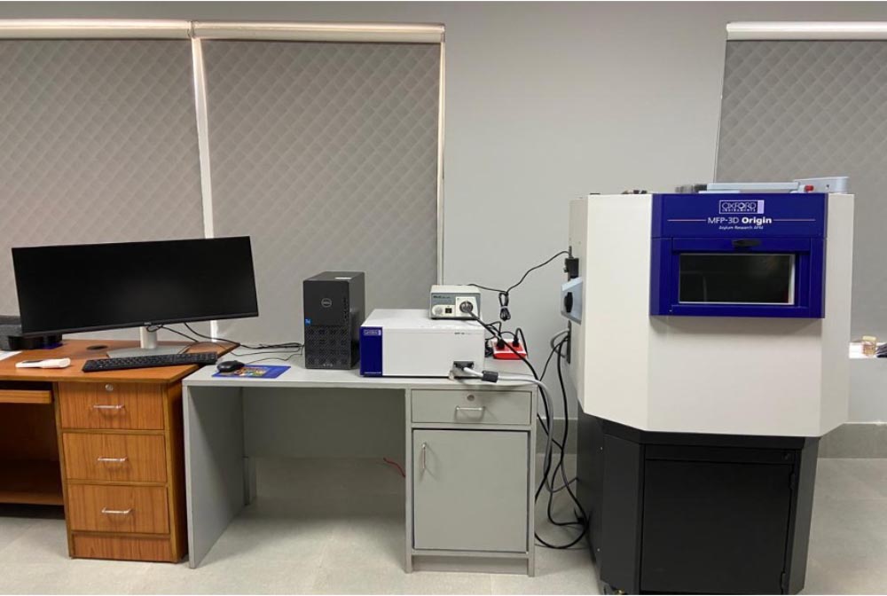
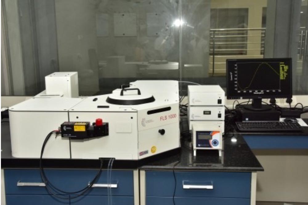
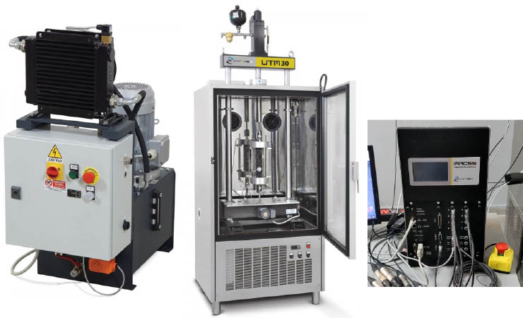
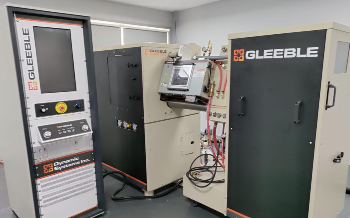
Photo Gallery