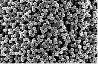
Model Name :
ZEISS EVO 18 SEM
EVO 18 Essential Specification :
Resolution
15 nm @ 30 kV 1 nA, LaB6
20 nm (15 nm) @ 1 kV SE and W (LaB6)
10 nm @ 3 kV SE
Acceleration Voltage : 0.2 to 30 kV
Probe Current : 0.5 pA to 5 µA
Magnification : < 5 – 1,000,000x
Field of View : 6 mm at the Analytical Working Distance (AWD)
X-ray Geometry : 8.5 mm AWD and 35° take-off angle
OptiBeam* Modes : Resolution, Depth, Analysis, Field of Fisheye
Pressure Range : 10 – 400 Pa with air or optionally water vapour
Available Detectors :
ETSE – Everhart-Thornley Secondary Electron Detector
BSD–Five Segment Diode Backscattered Electron Detector
EDS – Energy Dispersive Spectrometer
Chamber Dimensions : 365 mm (Ø) x 275 mm (h)
Future Assured Upgrade : BeamSleeve
Path Options :
Extended pressure kit (up to 3000 Pa)
Water vapour kit
Image Processing :
Resolution: Up to 3072 x 2304 pixels
Signal acquisition by integrating and averaging
Image Display :
High quality flat panel with SEM image displayed at 1024 x 768 pixels
Capable of dual channel display
System Control :
SmartSEM** GUI operated by mouse and keyboard
Multilingual Windows® 7 operating system
Utility requirements :
100 – 230 V, 50 or 60 Hz single phase
No water cooling requirement
US Keyboard, US control panel and mouse supplied
——————————————————————————————————————-
*OptiBeam – Active column control for highest resolution, largest field of view, or best depth of field
**SmartSEM – Fifth generation SEM control Graphical User Interface
Application
Scanning Electron Microscopy (SEM) is widely used to investigate the microstructure and chemistry of a range of materials. A SEM scans a focused electron beam over a surface to create an image. The electrons in the beam interact with the sample, producing various signals that can be used to obtain information about the surface morphology and composition. In addition to morphological, topographical and compositional information, a Scanning Electron Microscope can detect and analyze surface fractures, provide information in micro-structures, examine surface contamination, reveal spatial variations in chemical compositions, provide qualitative chemical analyses.
- Morphology and grain analysis
- Micro / Nanostructural analysis
- Elemental analysis
- Mapping of Elements in the sample
- Grain boundary and materials Study


CHARGES
| User type | KIIT Users | Academic & Research Institutions | Govt. Institutions | Govt. Industry |
|---|---|---|---|---|
| Charges in INR (per sample) SEM + EDS | 50 | 250 | 500 | 750 |
Sample Requirement
- Sample must be zero moisture content.
- Sample width should be below 10mm diameter and height should not be more than 8 mm.
- Mounting material should be conducting
Faculty In-Charge
 Name of the In-charge : Dr. Tapas Ranjan Sahoo
Designation : Associate Professor
Contact details : trsahoofch@kiit.ac.in
 Name of the In-charge : Dr. Jatin Sinha
Designation : Associate Professor
Contact details : jatin.sinhafch@kiit.ac.in
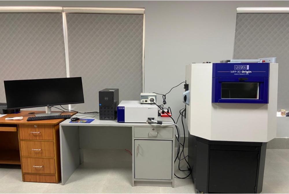
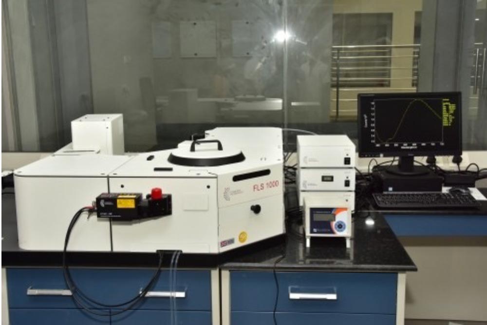
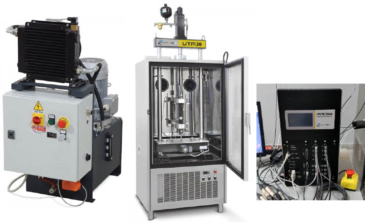
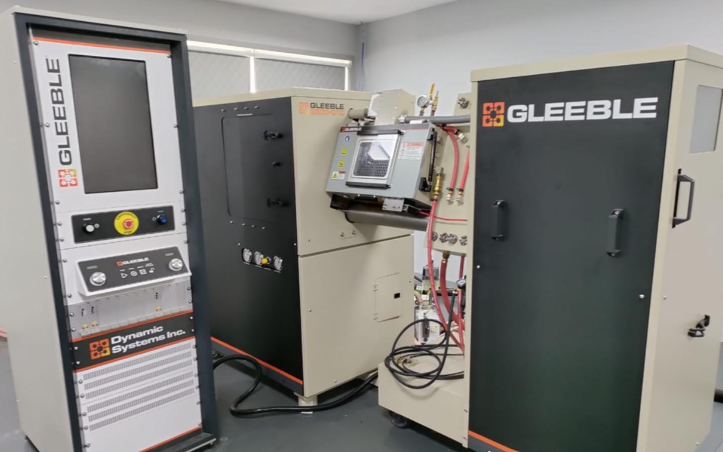
Photo Gallery