

Curabitur non nulla sit amet nisl tempus.
Model Overview.
Scanning Electron Microscopy (SEM) is a powerful technique for high-resolution imaging and compositional analysis of materials. It enables detailed study of surface morphology, microstructure, and elemental composition for research and industrial applications.
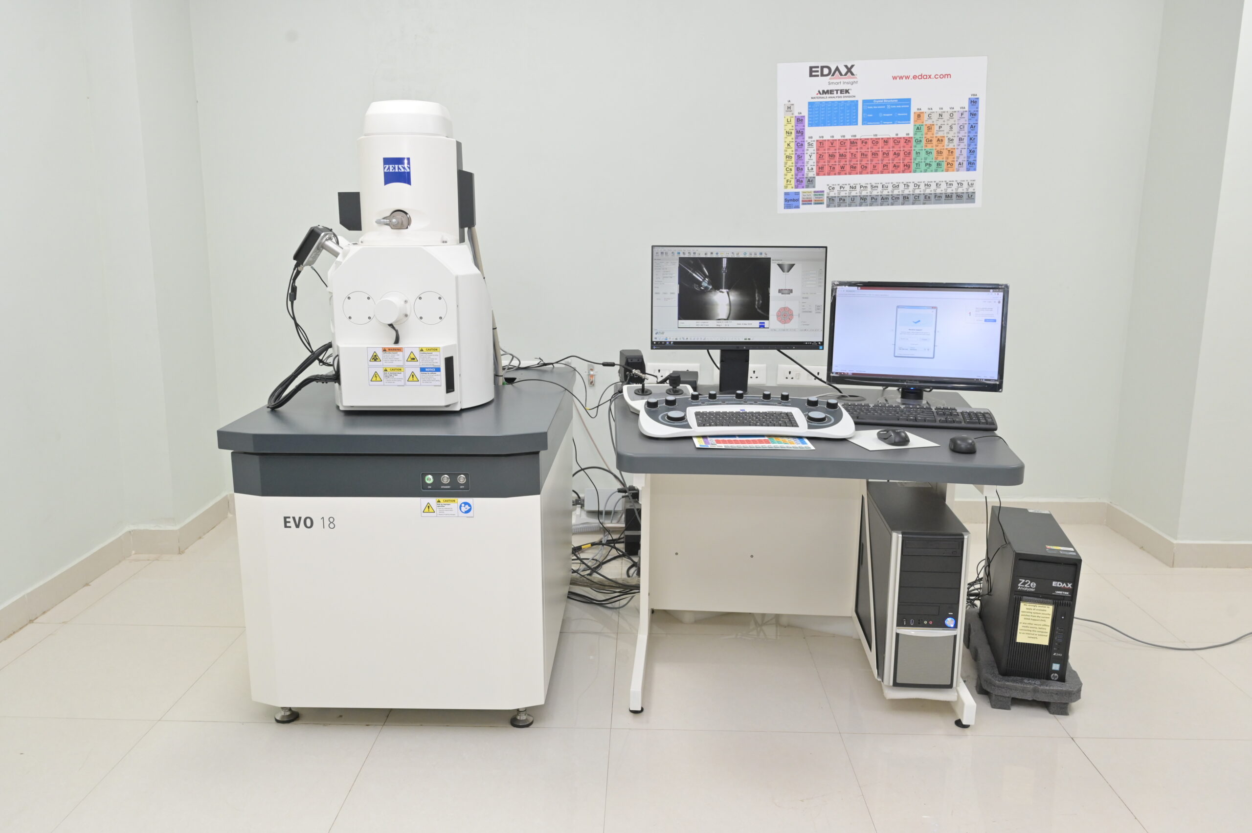
Model Details.
High-resolution electron imaging system
Resolution:
- 15 nm @ 30 kV, 1 nA (LaB6)
- 20 nm (15 nm) @ 1 kV SE and W (LaB6)
- 10 nm @ 3 kV SE
Accelerating Voltage: 0.2 kV to 30 kV
Probe Current: 0.5 pA to 5 µA
Magnification: < 5X to 1,000,000X
Field of View: 6 mm at Analytical Working Distance (AWD)
X-ray Geometry: 8.5 mm AWD and 35° take-off angle
Pressure Range: 10 – 400 Pa (air / water vapour)
Detectors Available:
- ETSE – Secondary Electron Detector
- BSD – Backscattered Electron Detector
- EDS – Energy Dispersive Spectrometer
Chamber Dimensions: 365 mm (Ø) × 275 mm (h)
Motorized multi-axis stage
High vacuum and variable pressure operation
Digital imaging and analysis software
SEM is an advanced imaging technique used for detailed surface morphology and compositional analysis at micro to nanoscale.
Key Applications:
Materials Study
- Surface morphology and microstructure analysis
- Fractography and failure analysis
- Grain size and phase distribution
- Nanomaterials and composite characterization
Materials Testing
- Elemental composition analysis using EDS
- Coating thickness and surface defects evaluation
- Particle size and shape analysis
- Corrosion and wear analysis
Process & Research Applications
- Metallurgical studies and alloy characterization
- Semiconductor and electronic materials analysis
- Powder metallurgy and ceramics
- Biological and environmental sample imaging
The Scanning Electron Microscope (SEM) provides high-resolution imaging of material surfaces with excellent depth of field. It enables detailed analysis of surface morphology, microstructure, and elemental composition using EDS. SEM is widely used for failure analysis, particle characterization, coating evaluation, and advanced research in materials science and nanotechnology.
