

Curabitur non nulla sit amet nisl tempus.
Model Overview.
Field Emission Scanning Electron Microscopy (FESEM) is an advanced, high-resolution imaging technique used to obtain detailed surface images and microstructural information of materials, making it an essential tool in nanotechnology, materials research, electronics, biology, and industrial quality control.
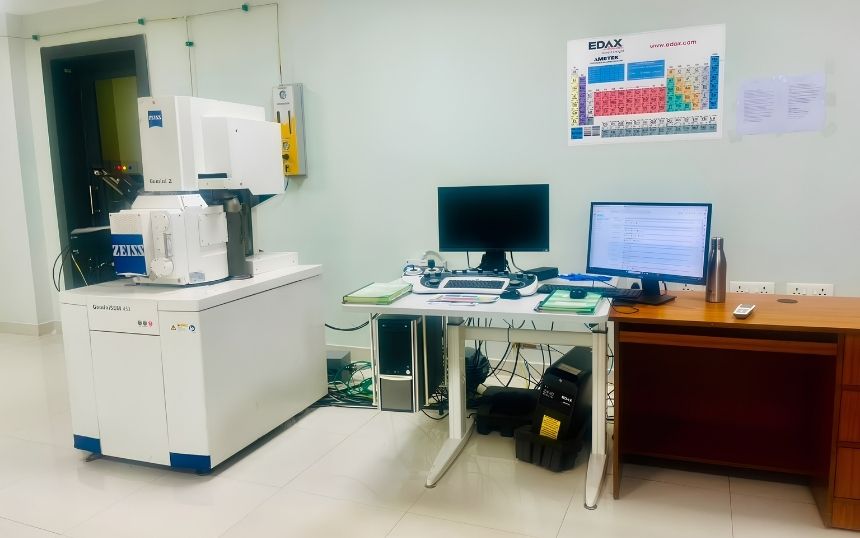

Model Details.
Specification2026-07-08T06:07:47+00:00
- Acceleration voltage Range – 0.02 -30 KV
- Resolution 1.5 nm @200 V
- Filament – Schottky field emitter
- Adjustment – Continuously variable in 10volt steps.
- Probe current – 40 nA configuration – 3 pA – 40 nA
100 nA configuration – 3 pA – 100 nA
300 nA configuration – 3 pA – 300 nA
- Magnification – 12x – 20,00000x reference to polaroid 5” *4.5” image format.
- Objective lens – Gemini II electromagnetic objective lens.80 degree conical final- lens with water cooling including double condenser lens.
- Working Distance -range 0.1 mm – 50 mm.
- Specimen chamber – 330 mm inner diameter
270 mm height
- Specimen stage – 5 axes motorized eucentric,controlled fromsmartSEM user interface,operated by a dual joystick control box.
Application2026-07-08T06:09:12+00:00
Field Emission Scanning Electron Microscopy (FESEM) is used for ultra-high-resolution surface topography analysis and nanoscale material characterization .
Key Applications:
Materials Study
- Analysis of surface morphology and microstructure
- Grain size and phase distribution studies
- Fracture and failure analysis of metals, ceramics, and polymers
- Investigation of coatings and thin films
- Characterization of nanoparticles, nanowires, nanotubes, and quantum dots
Key Advantages of FESEM
- Very high resolution (nanometer-scale imaging)
- Greater depth of field than optical microscopy
- High-quality surface imaging
- Capability for elemental analysis when coupled with EDS/EDX detectors
Capability of FESEM2026-07-08T06:10:47+00:00
- Ultrahigh resolutions imaging
- High Magnification
- Surface Morphology Analysis
- Imaging of Non-Conductive Materials
- Elemental Analysis
- Large Depth of Field
- Low Voltage Imaging
- Failure and Defect Analysis
